Winonics offers a complete range PCB solutions to bring leading edge applications and new technologies to market. Our products and technology focus is guided by our mission to deliver “Exceptional Service and Innovative Solutions, with No Boundaries”.
Multilayer Rigid and Rigid-Flex Printed Circuit Boards
Winonics is an industry leading manufacturer of Multilayer PCBs. Conventional Multilayer PCBs range from 3 to 24 layers, use conventional drilling and plating technologies and are single lamination constructions. Our conventional multilayer PCB capabilities are served by decades experience from a diverse team of engineers, specialists, experts, and operators.

Capabilities:
- Layer count 24+
- Panel Size up to 21”x24”
- Mixed Materials
- High Aspect Ratio
- Backdrilling
- Edge plating
- RF Microwave
- Cavities, countersunk holes or depth milling
- Heavy copper
- Controlled impedances
- All Surface Finishes
Ultra Fine Pitch PCB
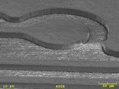
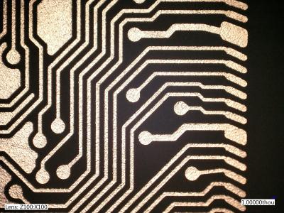
Winonics provides engineering and manufacturing support for Fine Pitch and Ultra-Fine Pitch PCBs used in high-density applications.
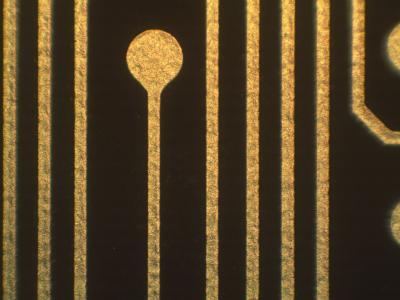
Fine Pitch PCBs are characterized by finer pitch features including narrower conductor widths and spacing that are required for designs using ultra-fine pitch BGAs and higher I/O count components.
Winonics capabilities include traditional dog bone fanouts as well as advanced technology via in pad construction. Via in pad technology enables much tighter routing required for Ultra-Fine Pitch BGAs devices.

Capabilities:
- Engineering and Manufacturing support for Ultra-Fine Pitch PCB designs
- Via in pad enabled fanouts
- Conductor widths down to 75µm
- Conductor widths below 50µm utilizing ACT-SAP advanced manufacturing technologies
High Density and Ultra-High Density Interconnects (HDI/UHDI)
Winonics supports High Performance, HDI/UHDI solutions for complex advanced technology applications.
HDI/UHDI PCBs are characterized by higher density attributes when compared to conventional PCBs, including laser microvias, sequential lamination construction, finer lines and spacing, and high-performance thin materials.
HDI PCBs take advantage of the latest manufacturing technologies available to enable the use of fine pitch and ultra-fine pitch BGA components that can increase functionality using the same or less surface area, facilitate miniaturization, and improving signal integrity. This advancement in PCB technology supports advanced features in groundbreaking new products, including 5G communications, networking equipment, medical patient monitoring, autonomous applications, remote sensing systems, vehicle-to-everything communications, and military applications such as satellites, avionics, and intelligent munitions.

Capabilities:
- Sequential laminations
- Stacked and staggered microvias
- Blind and Buried microvias
- Copper-filled microvias
- Minimum conductor widths and spacing
- Advanced technology materials
- Cavities, countersunk holes or depth milling
- Controlled impedances
RF, Microwave, Millimeter Wave
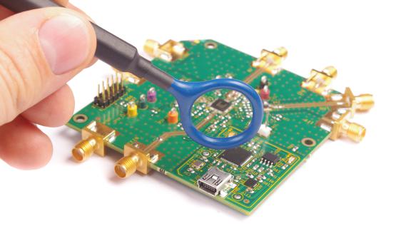
Winonics provides innovative engineering solutions and advanced process capabilities for RF, Microwave, and mmWave PCBs with frequency bands to support applications from defense, space, and aerospace electronics, complex telecommunications equipment, to 5G enablement, and mmWave automotive radar.
Our Engineering and Manufacturing teams have extensive experience with a wide range of low-loss and high-speed laminate materials to ensure that your designs meet DFM/DFX standards for quality, performance, and reliability in the field.
Capabilities:
- Tight tolerances for critical RF features
- Uniform copper build-up
- Mechanical Backdrilling
- High-performance materials including Rogers, Taconic, Panasonic, and Isola
- IPC class 2, IPC class 3
- AOI, Flying Probe, Differential Impedance, & TDR testing
Additive Technologies, ACT-SAP
Winonics and its parent company Additive Circuits Technologies, LLC are jointly developing commercial applications for Fully Additive and Semi-Additive Process (ACT-SAP) manufacturing technologies in our Advanced Research and Development Center located in the Winonics facility in Brea, CA. The department is staffed with a highly specialized team of engineers and technicians that has set their sole focus on furthering ACT’s pioneering technologies for manufacturing next generation printed circuit boards and microelectronics.
Partnerships and Program Opportunities
If Innovation is the driving force, the core competency of the ACT™ group is the development and commercialization of new manufacturing solutions to support our customer’s current NPI programs and forward-looking technology roadmap and implementing these into a scalable production platform and successful market launch.
ACT™ and Winonics uses state of the art equipment, processes, engineering, and innovative solutions in order to break down barriers and deliver new technology milestones.
We know that new products and technologies will lead to rapid success in the market and in order to ensure that you meet your Program objectives and timelines, dedicated resources from ACT™ and Winonics are assigned to your projects.
For more information on NPI Programs, R&D Partnerships, or to contact the ACT™ team: technologysolutions@winonics.com
ACT-SAP Capabilities Matrix and Technology Roadmap
| Feature | Current ACT-SAP | Advanced ACT-SAP | Future ACT-SAP |
|---|---|---|---|
| Outer Layer Trace/Spacing | 35µm / 35µm | 25µm / 25µm | 10µm / 10µm |
| Inner Layer Trace/Spacing | 35µm / 35µm | 25µm / 25µm | 10µm / 10µm |
| Minimum PCB Thickness | 100µm | 100µm | 100µm |
| Maximum Copper Build-up | 35µm | 35µm | 35µm |
| Minimum Copper Build-up | 2µm | 2µm | 2µm |
| Tolerance of Copper Conductor Dimensions | ± 10% | ± 10% | ± 10% |
| Circuitry Attributes | ACT-SAP |
|---|---|
| ✓ Ultra-fine pitch/high density circuitry | Y |
| ✓ Ultra-thin conductor build-ups | Y |
| ✓ Advanced designs at near zero tolerances | Y |
| ✓ Precise trace/pad geometries | Y |
| ✓ Uniquely high bond strength | Y |
| ✓ Improved signal integrity characteristics | Y |
